The Basics of Semiconductor Technology
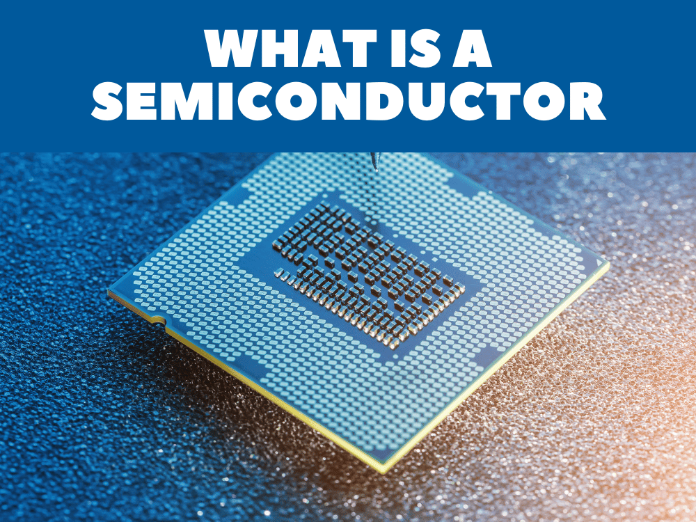
Blog Introduction: A semiconductor is a material that possesses electrical conductivity between that of an insulator and a conductor. It is used in many electronic devices and is essential for modern technology. In this blog post, we will discuss the basics of semiconductor technology and how it works.
How Semiconductors Work
Semiconductors are materials made up of elements from group 3A to group 5A on the periodic table, such as silicon and germanium. These materials have unique electrical properties in which their conductivity can be altered by adding impurities or doping agents into their structure. By adding these impurities, electrons can be either added or removed from the material, creating an excess or shortage of charge carriers within its lattice structure. This means that semiconductors can act as either an insulator (blocking current) or a conductor (allowing current).
The two types of semiconductors are called n-type (where there is an excess of electrons) and p-type (where there is a shortage of electrons). When these two types are combined together, they form a diode that allows current to flow in one direction only – usually from the n-type to the p-type material. Diodes are often used in applications such as voltage regulation or rectification (for example, AC-DC power supplies).
Semiconductor Manufacturing
Semiconductors are manufactured using lithographic techniques which allow patterns to be etched onto a substrate using light sources with different wavelengths. This process allows features to be created with incredibly small dimensions – down to 10 nanometres. The use of light sources also allows higher resolutions than those achievable with other methods such as photomasking. After etching, metal contacts are then deposited onto the substrate to create the complete device.
Conclusion
In summary, semiconductors are materials that possess electrical conductivity between that of an insulator and a conductor and are used in many electronic devices today. They work by adding impurities into their structure which alters their conductivity levels depending on whether they become n-type or p-type materials. Currently, they are manufactured using lithographic techniques which allow features to be created with incredibly small dimensions – down to 10 nanometres – allowing for better resolution than other methods available today. Hopefully, this overview has given you some insight into semiconductor technology and its applications!


